25 jun 2026
IBM claims world’s first sub-1 nanometer chip technology

A new chip architecture from IBM can integrate nearly 100 billion transistors on a chip the size of a human fingernail - nearly twice the transistor density of the company’s previous generation of chip technology. The resulting improvement in chip compute performance and energy efficiency comes from what IBM describes as the “world’s first sub-1 nanometer chip technology” for AI data centers. “It's not just an incremental step, it's a meaningful leap forward,” said Jay Gambetta , director of IBM Research and IBM Fellow, in an advance media briefing.
across the coverage
IBM has developed a sub-nanometer (nm) chip technology it says could be used to produce commercial chips within five years, and has mapped a path to 0.1 nm. Big Blue claims its new process node can cram nearly 100 billion transistors onto a silicon die the size of a fingernail, almost double the density of the 2 nm technology it unveiled back in 2021. The new process as disclosed is actually for 0.7 nm or 7 Angstroms (7A), compared with the cutting-edge manufacturing nodes now being prepared for production in 2028 by the likes of Intel and TSMC which are 1.4nm, or 14 Angstroms.
the register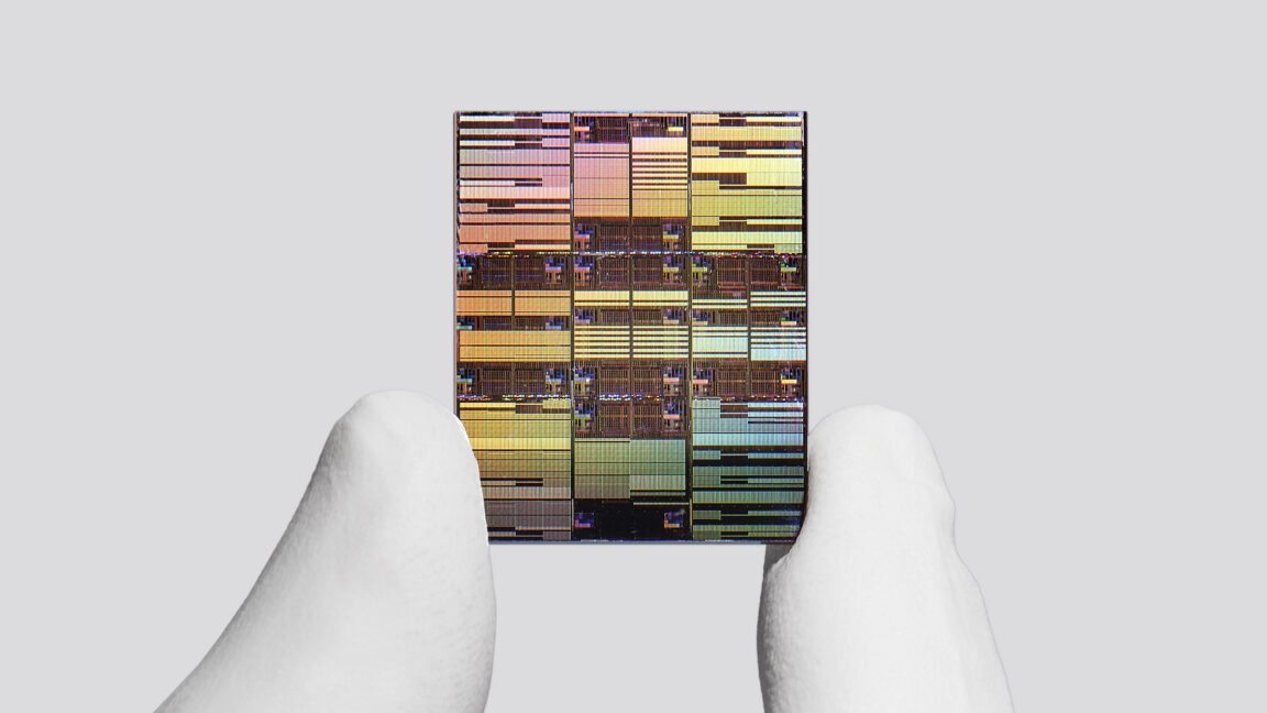
coverage · 2 outlets
- 10:03the register
IBM stacks up a sub-nanometer chip future
sitrep links out to every source. metadata only, no article text is stored here.